PCells and custom devices
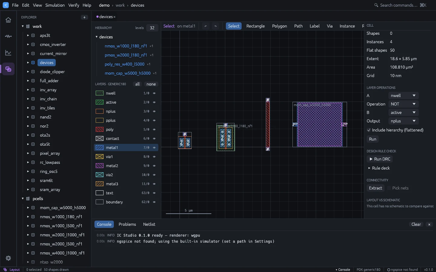
IC Studio has six built-in parametric cells (PCells). They are drawn by code from the technology, so the same parameters give a correct device in generic180, SKY130 or any other PDK. For devices the built-in PCells cannot draw (non-rectangular active, special contact arrangements, bent or 45° gates), write a generator in SKILL: see Your own device generators.
Built-in PCells
| Kind | Parameters | Defaults | Terminal labels | Draws |
|---|---|---|---|---|
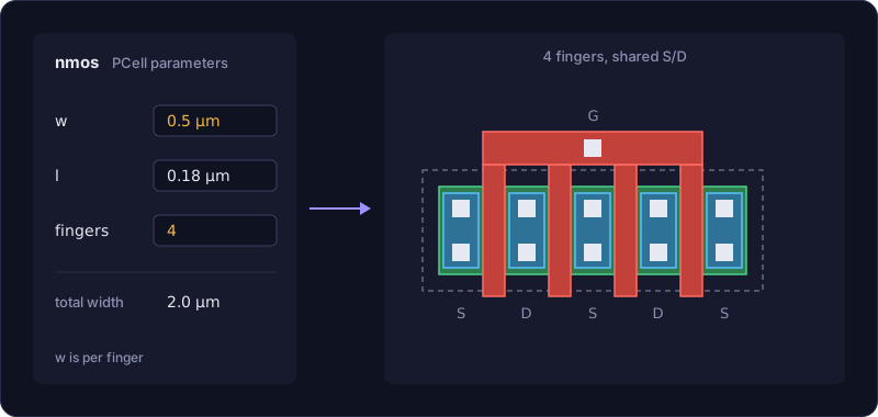
nmos | W, L, fingers, device | W 1 µm, L 0.18 µm, 1 finger | S, D, G | Active, poly fingers with a poly contact head, diffusion contact columns, n+ implant, PDK marker layers |
pmos | W, L, fingers, device | W 2 µm, L 0.18 µm, 1 finger | S, D, G | As nmos, plus p+ implant and an nwell |
poly_res | W, L | W 0.4 µm, L 5 µm | A, B | Poly body with a poly contact at each end, resistor marker layers |
mom_cap | W, H | 5 µm x 5 µm | BOT, TOP | metal1 bottom plate and metal2 top plate with a tab each, capacitor marker layers |
ntap | H | 1 µm | B | n+ tap in an nwell (PMOS bulk), one contact column wide |
ptap | H | 1 µm | B | p+ substrate tap, one contact column wide |
- W is per finger. An
nmoswith W 1 µm and 2 fingers is two 1 µm transistors in parallel (total width 2 µm); fingers alternate S / D / S. Extraction reports one device per finger, and LVS merges parallel devices. - Device appears when the technology is a PDK with several MOS devices of that polarity (for example low- and high-Vt variants). The PCell then draws that device’s marker layers and the variant name ends with the device name. The default is the PDK’s first device.
- Lengths snap to the technology grid. The origin is the lower-left corner of the active (MOS, taps), of the resistor body or of the bottom plate.
ntapandptapare not in the placement palette: schematic-driven layout creates them, and the MCP toolplace_pcellaccepts them.
Placing and changing PCells
| Where | How |
|---|---|
| Layout editor | Press I, pick the PCell in the left panel, set its parameters, click to place |
| Inspector | Select a placed PCell, edit the parameters in the PCell section, press Apply |
| Schematic-driven layout | Verify > Generate Layout from Schematic places every MOS as a PCell sized from the schematic (see Schematic-driven layout) |
| Generators | Layout Generators > Matched Placement and By Example place PCell units (see Tools) |
| MCP | place_pcell (see below) |
place_pcell takes sizes in µm:
{
  "cell": "work/amp",
  "kind": "nmos",
  "params": { "w": 2, "l": 0.5, "fingers": 4 },
  "x": 0, "y": 0, "rot": 0,
  "name": "M1"
}
Name MOS instances after their schematic devices (M1) so that flylines and LVS can pair
them.
How variants are stored
Each parameter set is generated once and stored as an ordinary cell in the pcells
library, named after its parameters in dbu:
| PCell | Variant name |
|---|---|
nmos W 1 µm, L 0.18 µm, 2 fingers | nmos_w1000_l180_nf2 |
the same with PDK device sky130_fd_pr__nfet_01v8_lvt | nmos_w1000_l180_nf2_sky130_fd_pr__nfet_01v8_lvt |
poly_res W 0.4 µm, L 5 µm | poly_res_w400_l5000 |
mom_cap 5 µm x 5 µm | mom_cap_w5000_h5000 |
ntap H 1 µm | ntap_w1000 |
Placing the same parameters again reuses the variant. Apply in the inspector points the
instance at another variant; the old variant stays in pcells (delete it from the project
tree when nothing uses it).
A variant’s cell.json keeps its parameters ("pcell": {"kind": "mos", ...}) next to the
layout, so hierarchy, GDS export, DRC and extraction treat it as a normal cell. When the
technology is replaced (Tools > Load PDK, ics load-pdk) every variant is regenerated
from its parameters, as long as the database unit stays the same. Do not edit a variant’s
layout by hand: the edit is lost on the next regeneration. Copy it to another library
first, or write a generator.
What the technology must provide
PCells draw only from the technology, so a new PDK needs these entries (see Technology):
| Entry | Used for |
|---|---|
roles: diffusion, tap, poly, nwell, nimplant, pimplant | The layers each PCell draws |
roles: diff_contact, poly_contact | The vias for S / D columns, tap contacts and poly heads |
Layer min_width, min_spacing, min_area | Minimum W and L, contact plate size, gate-to-contact distance |
rules: gate_contact_space, poly_endcap, implant_enc, nwell_enc, marker_enc | Spacings and enclosures inside the device |
[[device]] layers | Marker layers of each MOS device |
[[resistor]] / [[capacitor]] layers | Marker layers of poly_res (resistor on the poly layer) and mom_cap (capacitor between metal1 and metal2) |
[[pcell_layer]] | Any further layer, drawn around poly_contact, diff_contact, gate, diffusion, poly or a named layer, optionally only for some kinds |
Parameters the technology cannot build are refused with a message such as
width 150 is below the minimum 220 (active width / one contact) or
gate length 100 is below the poly minimum width 150. The PDK tests check that every
PCell of SKY130 and IHP SG13G2 is DRC clean; do the same for a new PDK by placing each
PCell and running DRC.
Device shapes extraction understands
Devices are recognised from geometry, not from the PCell parameters, so any layout that draws a transistor the way the rules below expect is extracted and compared by LVS, whether it came from a PCell, a SKILL script, GDS import or hand drawing.
| Shape | W and L |
|---|---|
| Rectangular gate on rectangular active | L across the gate between source and drain, W = area / L |
| Non-rectangular active (L-, U- or T-shaped) with straight gates | As above for each gate. One poly crossing both arms of a U makes two transistors with a shared gate |
| Bent gate (poly turning a corner over the channel, also U-shaped gates) | L = area / mean edge (the mean of the source and drain edge lengths); W = the mean edge, less a share of the corner squares set by bend_corner |
| Ring gate (enclosed layout transistor) | As a bent gate: W is the mean of the inner and outer perimeter |
| 45° or any-angle active or poly | As a bent gate, measured on the exact any-angle geometry |
| Instances rotated by 90° multiples or mirrored | As drawn |
A gate that is not a rectangle must split the diffusion into exactly two pieces (source and
drain); otherwise it is skipped with the warning
gate ... does not separate two diffusion pieces. For connectivity, any-angle shapes on
every layer are replaced by a staircase of narrow bands (a grid step, at least 10 dbu), so
wires and contacts on them connect as drawn; device sizes always use the exact geometry.
Resistors follow the same rules: an L-shaped or 45° resistor body must join exactly two terminal pieces, and its squares are L / W measured like a bent gate. Capacitor areas and perimeters near any-angle shapes are exact.
Bend correction. Counting each corner square of a bent gate fully (W = mean edge) is the
first-order estimate. Foundry decks often count a corner as about half a square; set
bend_corner in the PDK [rules] to match:
[rules]
bend_corner = 0.5   # 1 (default): W = mean edge; 0: W = the shorter (inner) edge
With 0.5, the L-shaped gate above (edges 2.82 and 3.18 µm, L 0.18 µm) has W = 2.91 µm.
DRC checks any-angle geometry too: near any-angle shapes, width, space, separation,
enclosure and extension are measured on the exact polygons, edge to edge in the
Euclidean metric, so a 45° wire at the minimum width and spacing is clean. Distances within
3/4 dbu of the limit pass (any-angle vertices are rounded to the grid), and acute corners
are reported. The other rules see the staircase (see Verification).
The built-in PCells always draw rectangular active. For an L- or U-shaped device, use a generator.
Your own device generators
User-defined PCells (pcDefinePCell) are not supported. A SKILL procedure that writes one
cell per parameter set does the same job: run it with Tools > Load SKILL (.il),
ics skill or the MCP tool run_skill, then place the generated cells with I
(Place cell) like any other cell.
This generator draws an NMOS whose active is L-shaped, with the source contact in a narrow vertical arm (generic180 layer names):
; NMOS with an L-shaped active: the source contact sits in a vertical arm.
procedure(nmosL(lib w l)
  let((name cv gx dx top)
    name = sprintf(nil "nmosL_w%d_l%d" round(w*1000) round(l*1000))
    cv = dbOpenCellViewByType(lib name "layout" "maskLayout" "w")
    gx = 1.0                     ; gate left edge
    dx = gx + l + 0.3            ; drain contact left edge
    top = w + 1.2                ; top of the source arm
    dbCreatePolygon(cv "active" list(0:0 dx+0.32:0 dx+0.32:w 0.42:w 0.42:top 0:top))
    dbCreateRect(cv "poly" list(gx:-0.25 gx+l:w+0.4))
    dbCreateRect(cv "nplus" list(-0.2:-0.4 dx+0.52:top+0.2))
    foreach(c list(list(0.1 top-0.32 "S") list(dx w/2-0.11 "D"))
      let((x y)
        x = car(c)  y = cadr(c)
        dbCreateRect(cv "contact" list(x:y x+0.22:y+0.22))
        dbCreateRect(cv "metal1" list(x-0.06:y-0.06 x+0.28:y+0.28))
        dbCreateLabel(cv "metal1" x+0.11:y+0.11 caddr(c) "centerCenter" "R0" "roman" 0.1)))
    dbCreateLabel(cv "poly" gx+l/2:w+0.3 "G" "centerCenter" "R0" "roman" 0.1)
    name))

foreach(p list(list(1.0 0.18) list(2.0 0.5))
  printf("%s\n" nmosL("mylib" car(p) cadr(p))))
ics skill myproj nmos_l.il
ics extract myproj mylib/nmosL_w1000_l180   # M1 D G S sub nmos w=1u l=0.18u
ics drc myproj mylib/nmosL_w1000_l180       # 0 violation(s)
Tips:
- Cell names allow letters, digits,
_and-: encode sizes in nm (w1000), not1.0. - Mode
"w"clears the cell, so running the script again regenerates every variant. - Label the terminals on a routing layer (
metal1,poly): labels in a placed cell are local to it, but they name the nets inside the cell for LVS of the cell itself. - In point lists, write a negative coordinate after another point in parentheses,
1.5:1.5 (-0.3):1.5, or the minus is read as a subtraction. - Read rules from your PDK rather than hard-coding them, and check each variant with
ics drcandics extract.
Adding a built-in PCell kind
A new built-in kind is Rust code in crates/ics-core/src/pcell.rs:
- Add a variant to
enum PCellwith its parameters in dbu. - Extend
kind_name,variant_name,summaryandgenerate(write agen_*function that draws from the technology roles, vias and rules), anddefaultsif it belongs in the placement palette. - Add the parameter editor in
pcell_params(crates/ics-studio/src/layout_view/edit.rs) and the kind inpcell_fromand theplace_pcellschema (crates/ics-mcp/src/tools.rs). - If extraction should recognise it as a new device type, extend
extract.rsandlvs.rs. - Add tests: DRC clean in generic180 and in the PDK tests of
pdk.rs, and extraction of the generated layout.