Pixel optics
IC Studio models the optics of an image sensor pixel from its stack: microlens, colour filters, dielectrics and metal grid, anti-reflection films and the silicon photodiode. It gives the quantum efficiency (QE) of each Bayer colour, the optical crosstalk at a chief ray angle (CRA), where the light is lost, and the photocurrent for an illuminance, which goes straight into the pixel circuit’s simulation.
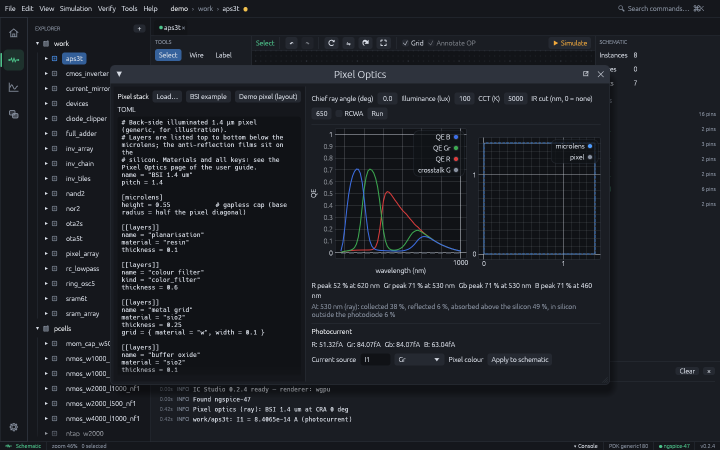
- GUI: Simulation > Pixel Optics… (or the command palette). Edit the stack, set the CRA and the illumination, Run, then Apply to schematic to write the photocurrent of a colour into a current source of the open cell (undoable).
- CLI:
ics pixel pixels/bsi_1p4um.toml --cra 20 --lux 100 --cct 5000, with--jsonfor the full result and--set PROJECT CELL I1 --color Grto write the photocurrent into a current source.--method rcwa [--harmonics 11]selects the rigorous solver.
Example stacks ship in pixels/: a back-side illuminated 1.4 µm pixel, a front-side
illuminated 2.8 µm pixel with three metal levels, and the demo 3T pixel read from its layout.
From the layout
A stack can take its pitch, metal patterns and photodiode from a pixel cell’s layout:
[layout]
cell = "aps3t"
boundary = "boundary"                 # the pixel frame; the pitch follows from it

[microlens]
height = 2.5
center = "photodiode"                 # or offset = [dx, dy] in µm

[[layers]]
name = "metal 1"
material = "sio2"
thickness = 0.5
pattern = { material = "al", layout = "metal1" }

[photodiode]
top = 0.1
bottom = 3.0
layout = "active not interact poly"   # diffusion without a gate
layout takes a technology layer or a derived-layer expression of the DRC deck syntax
(and, not, interact, inside, size, …). The shapes are clipped to the frame and
repeated in every pixel. Patterns can also be written directly as
rects = [[x0, y0, x1, y1], ...] (µm from the pixel’s corner). The photodiode area limits
collection laterally; light absorbed beside it is reported as lost. center = "photodiode"
shifts each microlens over the photodiode’s centre.
- CLI:
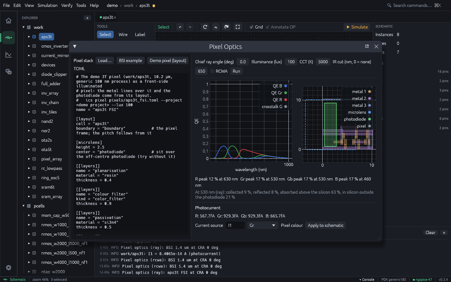
ics pixel pixels/aps3t_fsi.toml --project <project> --lux 100 - GUI: Demo pixel (layout) in the Pixel Optics window reads the open project. The plan view shows the patterns, the photodiode and the lens.
On the demo pixel, whose photodiode sits at the edge of the 10.2 µm pixel, centring the lens raises the green QE at 530 nm from 0.106 to 0.176.
From the PDK cross section
A technology can describe its back-end cross section (cross_section in a
PDK file; generic180 has one). The stack of a pixel cell
then follows from the PDK and the layout alone: the dielectric levels, the metals of each
level from their layout layers, the photodiode area, the colour filter, planarisation and
microlens, and the carrier diffusion in the silicon.
- CLI:
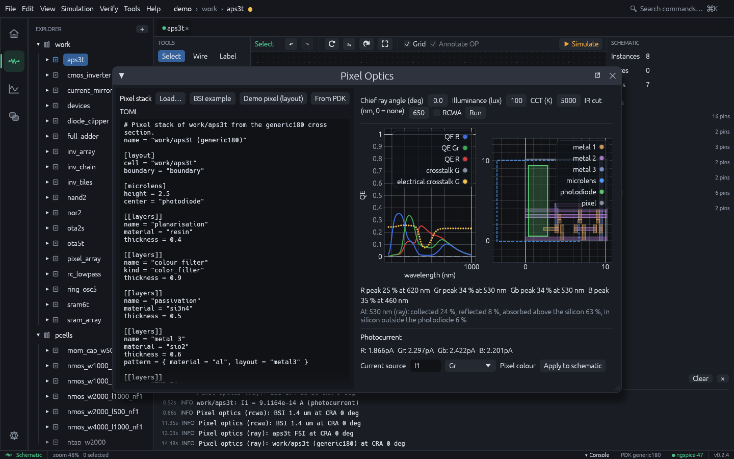
ics pixel --project <project> --cell aps3t --lux 100, or--emit-stackto print the generated stack and edit it. - GUI: From PDK in the Pixel Optics window (or Pixel stack of the open cell from the PDK cross section in the command palette) writes the open cell’s stack into the editor.
Two solvers
- Ray (default): geometric rays with thin-film optics on the silicon. Fast (under a second), gives per-lens optical crosstalk and a detailed light budget. Accurate while the pitch is well above the wavelength.
- RCWA (rigorous coupled-wave analysis): solves Maxwell’s equations over the 2 × 2 Bayer
cell, so it includes diffraction, interference in every layer and the near field of the
grid; use it for pixels around 1.5 µm and below. The microlens is staircased in 8 slices.
Accuracy grows with the harmonics per direction (
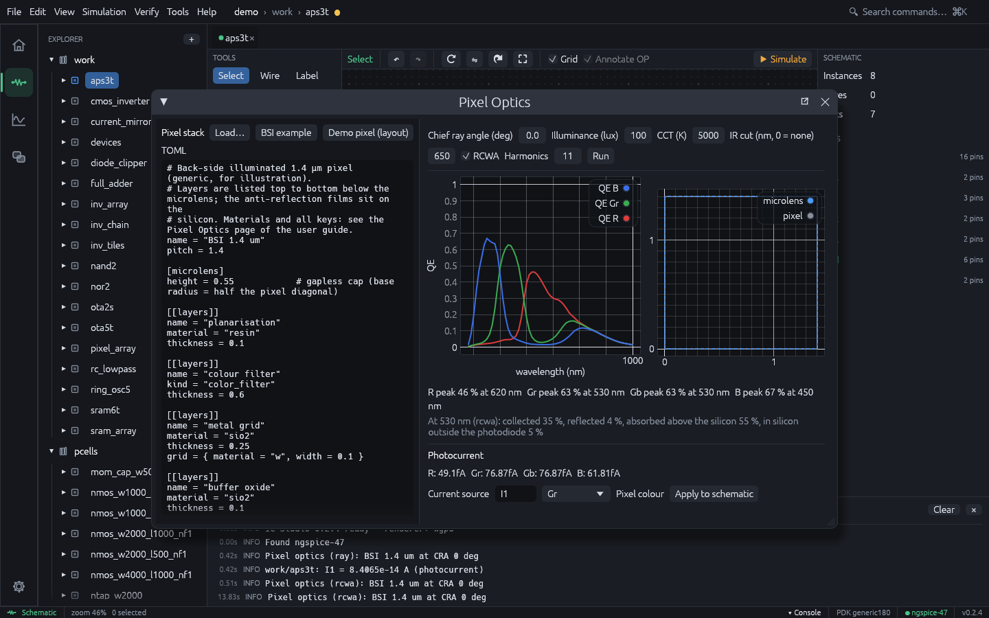
--harmonics, the Harmonics field): for the 1.4 µm example the green QE at 550 nm is 0.589, 0.596, 0.592 and 0.594 for 9, 11, 15 and 19 harmonics. 11 harmonics over 63 wavelengths take about 8 s on 10 cores. In-plane permittivities follow Li’s factorisation rules, so metal patterns converge; a pattern needs enough harmonics to resolve its smallest opening against the 2 × 2 cell. RCWA reports no per-lens crosstalk, and absorption above the silicon is one figure.
The solvers agree exactly without patterned layers (both reduce to thin-film optics); on the 1.4 µm example the ray model gives a green peak of 0.71 and RCWA 0.61, the difference being diffraction and interference at that pitch.
Carrier collection and electrical crosstalk
Without a [silicon] section, carriers count when they are generated inside the photodiode’s
box (its area and depth range). With one, they diffuse:
[silicon]
diffusion_length = 20     # µm, minority carriers in the neutral silicon
epi = 4.0                 # epitaxial layer: carriers reaching its bottom are lost
surface = "reflecting"    # or "recombining"
dti = { depth = 2.0, width = 0.1 }   # deep trench isolation on the pixel boundaries
# grid = 0.08             # voxel size (µm); default about pitch / 16
Each photodiode’s collection probability P(r) solves the diffusion equation ∇²P − P/L² = 0 over the 2 × 2 cell (P = 1 in its depletion region, 0 in the other photodiodes’, 0 at the epi bottom, no flux through the trenches), and its signal is the optical generation G(r) weighted by P, by reciprocity. Both solvers deliver G on the voxel grid. QE then includes the carriers that diffuse in from beside and below the photodiode, and the electrical crosstalk is reported per colour: of the carriers generated under a pixel and collected, the fraction a neighbour collects. It grows with wavelength, as red and near-infrared light is absorbed deep where carriers spread; trenches cut it.
With a very short diffusion length the model gives the box result again (checked in the tests for both solvers).
The ray model
Rays start uniformly over one 2 × 2 Bayer cell of an infinite array, as a plane wave at the chief ray angle. Each ray
- refracts at its pixel’s spherical-cap microlens (or between caps onto the lens base),
- passes the thick layers top to bottom, refracting at each interface and losing the Fresnel reflection; in the colour filter it is absorbed according to the filter it is in at each depth, so light crossing into a neighbour’s filter is filtered by that filter; metal grid lines stop it,
- enters silicon with the transmission of the anti-reflection films at its angle (coherent thin-film optics, s and p averaged),
- is absorbed along its path in silicon. Carriers generated between the photodiode’s top and bottom depth count for the pixel above the point of generation.
QE is carriers collected per photon incident on the pixel. Crosstalk is the fraction of the light entering through a pixel’s microlens that another pixel collects. The budget splits the light into reflected, absorbed in the colour filter, metal, other layers, silicon above the photodiode, collected, and silicon below it (or transmitted).
Limits of the ray model: geometric optics, so no diffraction (use RCWA for small pitches), no reflections back up from the grid or the silicon, no interference inside the thick layers. Neither solver models electrical crosstalk (carrier diffusion between photodiodes).
Stack file
name = "BSI 1.4 um"
pitch = 1.4                    # µm

[microlens]
height = 0.55                  # cap height
# radius = 0.99                # base radius; default half the pixel diagonal (gapless)
# material = "resin"

[[layers]]                     # thick layers below the lens, top to bottom
name = "colour filter"
kind = "color_filter"          # takes each pixel's filter
thickness = 0.6

[[layers]]
name = "metal grid"
material = "sio2"
thickness = 0.25
grid = { material = "w", width = 0.1 }   # lines centred on the pixel boundaries

[[arc]]                        # thin films on the silicon, top to bottom
material = "ta2o5"
thickness = 0.055

[photodiode]
top = 0.05                     # collection depth below the surface (µm)
bottom = 3.0

[color_filters]                # optional: own filter materials
# red = "my_red"

[materials.my_red]             # optional: own materials
# n = 1.6, k = 0.0, or a table of [wavelength µm, n, k] rows:
# table = [[0.40, 1.62, 0.30], [0.60, 1.60, 0.002], [0.80, 1.59, 0.0]]
ambient sets the medium above the lens (default air).
Materials
| Name | Data |
|---|---|
si | crystalline silicon at 300 K, M. A. Green (2008) |
sio2 | fused silica, I. H. Malitson (1965) |
si3n4 | K. Luke et al. (2015) |
hfo2 | M. F. Al-Kuhaili (2004) |
ta2o5 | L. Gao et al. (2012) |
w, al | A. D. Rakić et al. (1998) |
resin | generic microlens resin, n = 1.55 + 0.005/λ² |
cf_red, cf_green, cf_blue | generic pigment filters (passbands with a few % leakage, transparent in the near infrared) |
air | 1 |
Tabulated data come from the refractiveindex.info database (public domain), 0.30 - 1.20 µm.
The colour filters are generic shapes, not a vendor’s dyes: use measured n, k of your filter
materials for real designs.
Photocurrent
The illuminant is a blackbody at the colour temperature, scaled to the illuminance at the pixel with the CIE 1924 photopic curve; light above the IR-cut edge (default 650 nm, 0 for none) is removed. The photocurrent of a pixel is q ∫ QE(λ) E(λ) λ / (hc) dλ times its area.