From circuit to silicon
A schematic says what is connected. A layout says where everything physically is: the exact shapes the factory prints on the wafer. This chapter explains how chips are manufactured, how to read a layout, and why layouts must follow design rules.
How a chip is made
A chip is built on a silicon wafer in a sequence of several hundred process steps: oxidation, deposition, implantation, etching, polishing. The steps that make a pattern use photolithography: the wafer is coated with light-sensitive resist, exposed through a mask (a stencil of the pattern), developed, and then etched or implanted only where the resist is open.
Each mask is one layer of your layout. When you draw a rectangle on the poly layer,
you are drawing part of the poly mask.
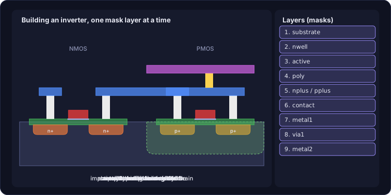
The animation builds the inverter from the CMOS logic chapter, one mask at a time:
| # | Layer | What the fab does with it | What it is for |
|---|---|---|---|
| 1 | substrate | (the starting wafer, p-type) | Body of every NMOS |
| 2 | nwell | Implants n-type dopant deep into the substrate | Body of the PMOS |
| 3 | active | Defines where silicon stays exposed; elsewhere thick isolation oxide grows | Transistors and substrate contacts |
| 4 | poly | Patterns polysilicon on the thin gate oxide | Gates (and short wires) |
| 5 | nplus / pplus | Implants n+ or p+ dopant into active not covered by poly | Sources and drains, taps |
| 6 | contact | Etches holes in the oxide above active or poly, fills them with metal | Connects metal1 down to silicon |
| 7 | metal1 | Patterns the first metal layer | Local wiring |
| 8 | via1 | Holes between metal1 and metal2 | Connects the metal layers |
| 9 | metal2, metal3 … | More metal layers | Longer, wider routing and power |
Self-aligned gates. Poly is patterned before the source/drain implant, so the gate itself blocks the implant: the source and drain end exactly at the gate edge. This is why, in layout, a transistor is simply poly crossing active. The channel length L is the width of the poly line; the channel width W is the width of the active under it.
Tools > Process Emulation in IC Studio runs a process flow on your own layout and draws the resulting cross-section along any cut line. See Process emulation.
Reading a layout
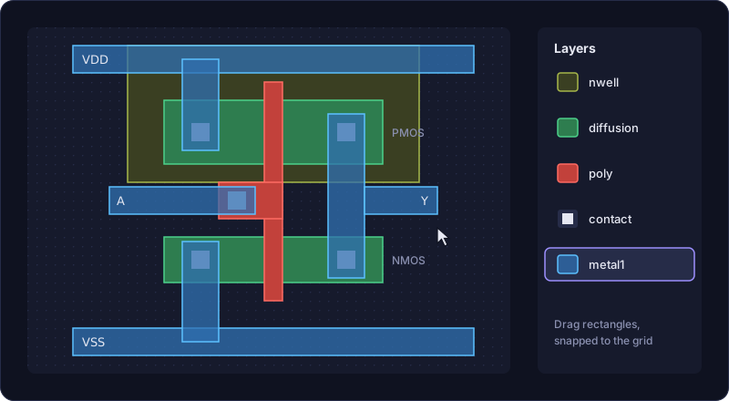
A layout is viewed from above, each layer in its own colour and fill pattern. The inverter in top view:
- Two horizontal strips of active (green): the NMOS at the bottom, the PMOS at the top inside the n-well.
- A vertical poly line (red) crosses both: it is the shared gate, the input.
- Contacts (white squares) on the active either side of the gate connect to metal1 (blue): the sources go to the VDD and ground rails, the two drains are joined to form the output.
- Taps: a p+ contact to the substrate (tied to ground) and an n+ contact to the n-well (tied to VDD) keep the bodies at the right voltage.
The Layout editor page explains each tool. Key facts:
- Layout coordinates are in database units: 1 dbu = 1 nm in the generic technology, and y points up.
- Labels on metal name the nets (
in,out,vdd), which extraction and LVS use. - The Layers panel shows each layer’s GDS number; hover a layer to see its minimum width and spacing.
Design rules
The factory cannot print arbitrarily small or close shapes: light diffracts, masks misalign, etches undercut. Its limits are written as design rules. The most common:
| Rule | Meaning | Example (generic 180 nm) |
|---|---|---|
| Width | Smallest size of a shape | poly ≥ 180 nm, metal1 ≥ 230 nm |
| Spacing | Smallest gap between two shapes on one layer | poly ≥ 240 nm, metal1 ≥ 230 nm |
| Enclosure | How far one layer must extend around another | active around a contact ≥ 100 nm |
| Extension | How far poly must stick out beyond active (the “end cap”) | so the gate cuts the channel completely |
| Area, density | Minimum area of a shape; fraction of the chip covered by a layer | for polishing (CMP) uniformity |
Shapes that break a rule may still be manufactured, but with a high chance of shorts or opens. A layout must be DRC clean (Design Rule Check) before tape-out.
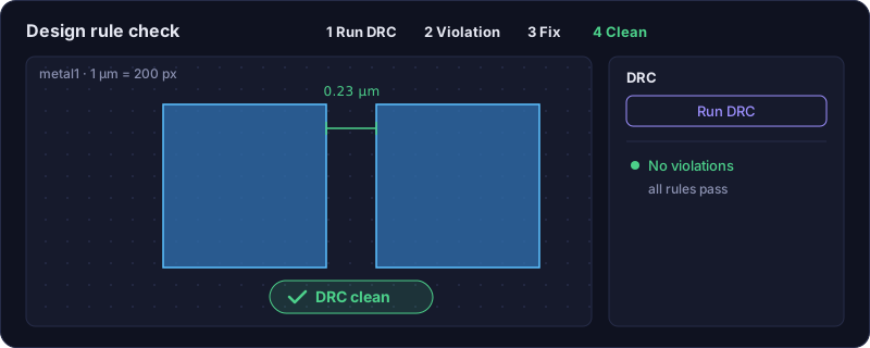
IC Studio helps while you draw: DRD shows the spacing halo of a shape being drawn, Magnet snaps shapes to exactly the minimum spacing, and Live DRC marks violations as they appear. See Verification.
LVS: is it the same circuit?
A DRC-clean layout can still be the wrong circuit: a missing contact, two nets accidentally shorted, a transistor of the wrong width. LVS (Layout Versus Schematic) extracts the circuit from the layout (transistors where poly crosses active, nets from connected metal) and compares it with the schematic, device by device and net by net.
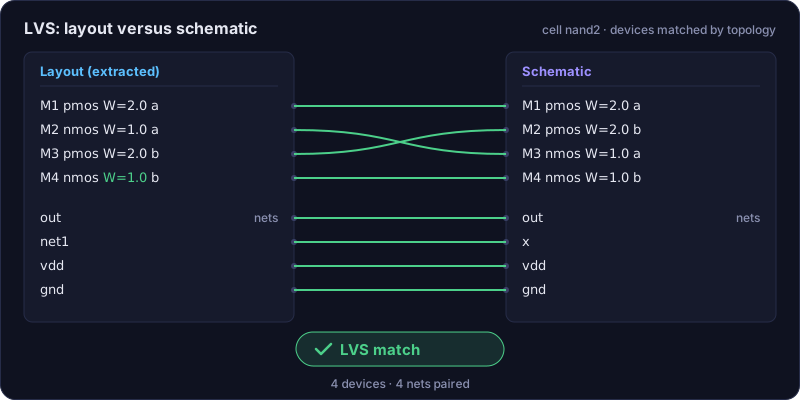
Two clean reports, DRC and LVS, are the minimum for any layout.
Parasitics: the wires are not ideal
In the schematic a wire is a perfect connection. In silicon it is a strip of metal with:
- resistance: a few hundredths of an ohm per square for metal, several ohms per square for poly (that is why long wires are drawn in metal, not poly);
- capacitance to the substrate below and to neighbouring wires (tens of aF per µm²);
- the junction capacitance of every source and drain.
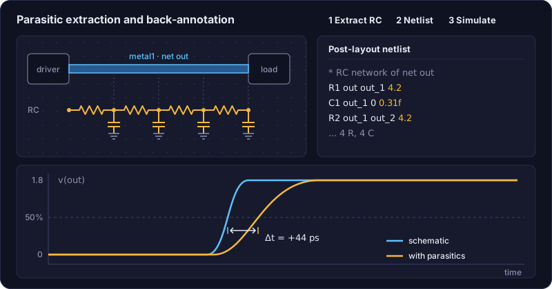
These parasitics slow circuits down. Parasitic extraction (PEX) computes them from the layout and adds them to the netlist, so a post-layout simulation shows the real speed.
Layout techniques you will see
- Shared diffusion: two transistors in series or with a common node share one source/drain region, saving area and capacitance. The generated layouts in IC Studio do this automatically.
- Fingers: a wide transistor is split into several parallel narrow ones side by side, which shortens the gate and reduces drain capacitance.
- Matching (analog): transistors that must be identical are interleaved
(
ABBA, common centroid) with dummies at the ends, so process gradients affect them equally. See Schematic-driven layout. - Guard rings and taps: rings of substrate or well contacts that collect stray currents and prevent latch-up, a parasitic thyristor in every CMOS process.
Schematic-driven layout
Drawing every rectangle by hand is slow. In schematic-driven layout the tool places the transistors of the schematic as PCells (parameterised cells that draw themselves from W and L), shows the connections still to make as flylines, and routes them.
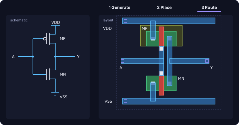
That is the flow of the next tutorial.
Try it: open the hand-drawn inverter of the demo:
ic-studio --demo --cell cmos_inverter --workspace layout
Find the active, poly, contacts and metal1 in the Layers panel; hide and show layers with the eye icons. Press Extract in the right panel and click a net in Nets to see which shapes form it. Press Run LVS: this layout has deliberate mistakes; click a difference to zoom to it.