CMOS logic
Digital chips are built from CMOS (complementary MOS) logic: every gate pairs NMOS transistors that pull the output down with PMOS transistors that pull it up. This chapter builds the inverter, then NAND and NOR, and explains what makes a gate fast or slow.
Transistors as switches
For logic, a MOSFET is a switch controlled by its gate:
| Gate = 0 (0 V) | Gate = 1 (VDD) | |
|---|---|---|
| NMOS | off | on |
| PMOS | on | off |
An NMOS passes a good 0 (it connects to ground well) and a PMOS passes a good 1 (it connects to VDD well). CMOS uses each for what it is good at: NMOS in the pull-down network to ground, PMOS in the pull-up network to VDD.
The inverter
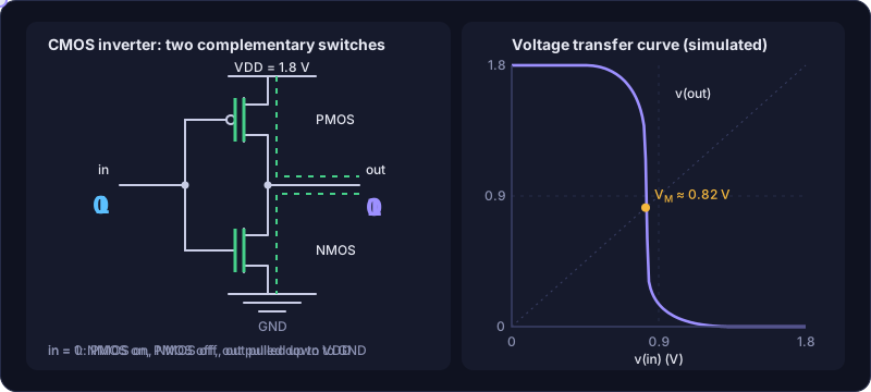
The simplest gate: one PMOS from VDD to the output, one NMOS from the output to ground, both gates tied to the input.
- in = 0: the PMOS is on, the NMOS is off. The output is connected to VDD: out = 1.
- in = 1: the NMOS is on, the PMOS is off. The output is connected to ground: out = 0.
In either steady state one of the two transistors is off, so no current flows from VDD to ground. A CMOS gate that is not switching burns (almost) no power. This single property is why CMOS won.
The voltage transfer curve
Sweep the input slowly from 0 to 1.8 V and plot the output: that is the voltage transfer curve (VTC), shown on the right of the figure (simulated in IC Studio with the generic technology, NMOS 1 µm, PMOS 2 µm, both 180 nm long).
- The output stays at 1.8 V for low inputs and at 0 V for high inputs: logic levels are restored, so noise does not accumulate through a chain of gates.
- In the middle the curve is very steep (a gain of about −55): small changes of the input around the threshold give large changes of the output.
- The switching threshold VM is where out = in. Here it is about 0.82 V, a little below the middle (0.9 V), because the NMOS is stronger than the PMOS.
- Noise margins: inputs below VIL ≈ 0.67 V are read as 0 and inputs above VIH ≈ 0.92 V as 1 (the points where the slope is −1).
Only while the input passes through the middle region are both transistors partly on, and a short-circuit current flows from VDD to ground (about 118 µA at the peak for this inverter).
NAND and NOR
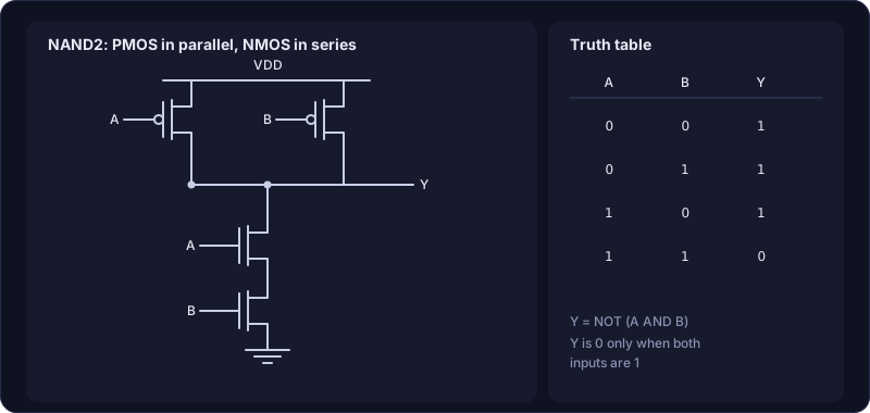
Every static CMOS gate follows one recipe:
- Build the pull-down network of NMOS transistors that conducts when the output should be 0. Series NMOS = AND; parallel NMOS = OR.
- Build the pull-up network of PMOS transistors as its dual: series becomes parallel and parallel becomes series.
| Gate | Output | Pull-down (NMOS) | Pull-up (PMOS) |
|---|---|---|---|
| Inverter | NOT A | one | one |
| NAND2 | NOT (A AND B) | two in series | two in parallel |
| NOR2 | NOT (A OR B) | two in parallel | two in series |
The output is always inverted: a single CMOS stage can only make inverting functions. An AND is a NAND followed by an inverter. NAND and NOR are each universal: any logic function can be built from either one alone.
Why designers prefer NAND to NOR: series transistors are slower (their resistances add). NOR puts the PMOS, already the weaker device, in series, so a NOR needs very wide PMOS to be fast. NAND puts the NMOS in series, which costs less.
Delay: why gates take time
A gate’s output drives a load capacitance CL: the gates of the next stages, the wires and its own drain junctions. Switching the output means charging or discharging CL through the transistor that is on, which acts like a resistor Ron. As in the RC circuit, that takes time:
t_p ≈ 0.69 · R_on · C_L
The propagation delay tp is measured from the input crossing 50 % of the swing to the output crossing 50 %. There are two of them: tpHL (output falling, through the NMOS) and tpLH (output rising, through the PMOS).
For the inverter above with a 20 fF load, IC Studio simulates tpHL ≈ 36 ps and tpLH ≈ 52 ps: rising is slower because the PMOS is weaker.
To make a gate faster, lower Ron (wider transistors) or lower CL (fewer or smaller gates to drive, shorter wires). But wider transistors also have larger gates, which load the stage before. Sizing is a balance.
Power
A CMOS chip burns power in three ways:
| Kind | Cause | Formula |
|---|---|---|
| Dynamic (switching) | Charging and discharging load capacitances | P = α · CL · VDD² · f |
| Short-circuit | Both transistors briefly on during an input transition | Small with sharp input edges |
| Leakage (static) | Transistors that are “off” still leak a little | Matters in advanced nodes |
α is the fraction of clock cycles the node switches. Because power goes with VDD², lowering the supply voltage is the most effective way to save power, which is why supplies have dropped from 5 V to below 1 V over the decades.
Sizing the transistors
The PMOS of the generic technology has k’ = 70 µA/V² against 280 µA/V² for the NMOS: it is four times weaker for the same W/L. Two common choices:
| PMOS width | VM | tpHL / tpLH | Comment |
|---|---|---|---|
| Wp = 2·Wn (2 µm) | 0.82 V | 36 / 52 ps | A common compromise: smaller, a bit unbalanced |
| Wp = 4·Wn (4 µm) | 0.90 V | 39 / 37 ps | Balanced: symmetric threshold and delays |
(Simulated with a 20 fF load. The balanced version has equal rise and fall delays, but its bigger PMOS also loads the stage driving it, so a 2:1 ratio is often the better choice inside a chain of gates.)
From the square law, setting the NMOS and PMOS currents equal at the switching point gives
V_M = (V_th,n + r · (V_DD − |V_th,p|)) / (1 + r), r = √(k'_p·W_p/L_p / (k'_n·W_n/L_n))
With Wp = 4·Wn, r = 1 and VM = VDD/2 exactly.
Try it: the demo has a ready-made inverter, NAND and NOR, and a ring oscillator:
ic-studio --demo --cell cmos_inverter --workspace simulation
Press F5 and look at the DC Sweep and Transient tabs. Then open nand2 and
nor2 (Explorer, or Ctrl+K), and ring_osc5: five inverters in a loop, which
oscillates because each stage’s delay keeps the loop from ever settling. Its period is
2 × 5 × tp.
Now build one yourself: Hands-on: design an inverter.