The MOSFET
Almost every transistor on a modern chip is a MOSFET: a metal-oxide-semiconductor field-effect transistor. This chapter explains what it is made of, how a voltage on its gate turns it on, and the few equations a designer actually uses.
Silicon and doping
Pure silicon conducts poorly. Its conductivity is set by adding tiny amounts of other elements, called doping:
- n-type silicon is doped with phosphorus or arsenic, which bring extra electrons (negative carriers).
- p-type silicon is doped with boron, which leaves holes (missing electrons that behave as positive carriers).
Heavily doped regions are written n+ and p+. Where n-type and p-type meet, a pn junction forms: a diode that conducts one way only. In normal operation the junctions of a MOSFET are reverse-biased, so they block current and isolate the transistor from the silicon around it.
The structure
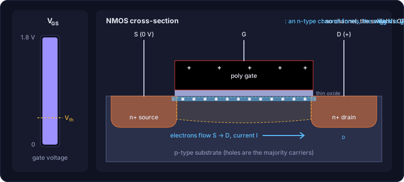
An NMOS transistor is built in p-type silicon (the substrate or body):
- two n+ regions, the source (S) and the drain (D);
- between them, a thin layer of insulating gate oxide (a few nanometres of SiO₂);
- on the oxide, the gate (G), made of polysilicon (“poly”) in older processes.
The gate, the oxide and the silicon under it form a capacitor. That is the whole trick.
How the gate turns it on
- Gate at 0 V. The source and drain are two n+ islands in p-type silicon, back to back diodes. No current flows: the switch is off.
- Gate voltage rising. The positive gate pushes the holes away from the surface, leaving a depletion region with no free carriers.
- Gate above the threshold voltage Vth. The gate now attracts enough electrons to the surface to invert it: a thin n-type channel connects source and drain. With a voltage between drain and source, electrons flow: the switch is on.
The higher the gate voltage above threshold, the more electrons in the channel and the more current. The amount by which VGS exceeds Vth is the overdrive voltage, Vov = VGS − Vth. It is the most important number in analog design.
No current flows into the gate. The gate is insulated by the oxide, so in DC it draws nothing. That is why MOS logic burns almost no power when it is not switching, and why one gate can drive many others.
The four terminals and the voltages that matter
| Terminal | Role | NMOS connection |
|---|---|---|
| Gate (G) | Controls the channel | Input signal |
| Source (S) | Where carriers come from | The lower voltage (often ground) |
| Drain (D) | Where carriers go | The higher voltage |
| Body / bulk (B) | The silicon underneath | Lowest voltage: ground |
Everything is described with voltages relative to the source: VGS (gate to source) and VDS (drain to source). The current through the channel is the drain current ID.
The three regions
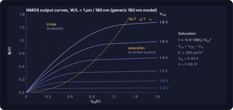
The output curves above are ID against VDS, one curve per gate voltage, simulated for the generic 180 nm NMOS. They show three regions:
| Region | Condition | Behaves like | Drain current |
|---|---|---|---|
| Cut-off | VGS < Vth | An open switch | ≈ 0 |
| Triode (linear) | VDS < Vov | A resistor controlled by the gate | k’·(W/L)·(Vov·VDS − VDS²/2) |
| Saturation | VDS ≥ Vov | A current source controlled by the gate | ½·k’·(W/L)·Vov²·(1 + λ·VDS) |
The dashed line VDS = Vov separates triode from saturation. In saturation the channel is “pinched off” near the drain, so the current hardly depends on VDS any more: the curves go flat. The small remaining slope is channel-length modulation, set by λ.
- Digital circuits swing between cut-off (switch off) and triode (switch on, a resistor).
- Analog circuits bias transistors in saturation, where they act as voltage-controlled current sources, the basis of every amplifier.
The square law
The saturation equation is called the square law:
I_D = ½ · k' · (W/L) · (V_GS − V_th)²
- k’ = µ·Cox is a process constant: how mobile the carriers are times the oxide capacitance per area. You cannot change it.
- W/L (width over length of the channel) is yours to choose. A wider transistor carries more current; a longer one carries less but is more ideal.
- Vth is set by the process: 0.45 V in the generic technology.
Real short-channel transistors deviate from the square law (velocity saturation, DIBL, subthreshold leakage); foundry models like BSIM4 capture this, and IC Studio’s built-in engine evaluates them. The square law is still the right way to think about a design: calculate with it, then check with the simulator.
A worked example
The generic NMOS has k’ = 280 µA/V² and Vth = 0.45 V. With W = 2 µm, L = 1 µm and VGS = 0.7 V:
V_ov = 0.7 − 0.45 = 0.25 V
I_D  = ½ · 280µ · (2/1) · 0.25² = 17.5 µA      (simulator: 18.7 µA, with λ)
You will meet this exact transistor again in the amplifier tutorial.
The PMOS: the complementary twin
A PMOS is the mirror image: p+ source and drain in an n-well (an n-type island in the p-type substrate), with holes forming the channel. Everything is reversed:
| NMOS | PMOS | |
|---|---|---|
| Channel carriers | Electrons | Holes |
| Turns on when the gate is | High (VGS > Vth) | Low (VGS < −|Vth|) |
| Source usually at | Ground | VDD |
| Body at | Ground (substrate) | VDD (n-well) |
| k’ (generic 180 nm) | 280 µA/V² | 70 µA/V² |
Holes are slower than electrons, so a PMOS carries about a quarter of the current of an NMOS of the same size in this technology. To match an NMOS, a PMOS must be made wider. That ratio is the subject of sizing.
On a schematic the PMOS is drawn with a small circle (a “bubble”) on its gate, a reminder that it turns on with a low input.
W, L and the parameters in IC Studio
In the schematic editor, a placed MOSFET (N for NMOS, P for PMOS) has the parameters:
| Inspector field | SPICE parameter | Default | Meaning |
|---|---|---|---|
| Model | model | nmos / pmos | Which device model (a PDK can offer several) |
| Width | w | 1u / 2u | Channel width W |
| Inductance / L | l | 180n | Channel length L |
| Multiplier | m | 1 | Number of identical devices in parallel |
The netlist line is M1 d g s b nmos w=1u l=180n. The generic models behind it are SPICE
level-1 (square-law) models:
.model nmos nmos (level=1 vto=0.45 kp=280u lambda=0.08 ...)
.model pmos pmos (level=1 vto=-0.45 kp=70u lambda=0.1 ...)
After an operating point simulation, the Operating Point results tab shows every MOSFET’s region (cutoff, triode, saturation), ID, VGS, VDS, Vth, gm and gds. Checking regions there is the first thing an analog designer does after every change.
Try it: plot the output curves yourself. Create a cell with one NMOS (W = 1u,
L = 180n), a voltage source on its gate and one on its drain, and ground on source and
body. Rename the sources VG and VD in the inspector’s Name field and give VG a
DC value of 1.2. In the Simulation workspace, enable DC Sweep of
VD from 0 to 1.8 and plot i(VD). You get the 1.2 V curve from the figure above
(the current comes out negative: SPICE counts current flowing into the source’s +
terminal). Then open Tools > Corner / Sweep Manager, add the variable VG.dc with the
values 0.8 1.0 1.2 1.4 1.6 1.8 and press Run Sweep: Overlay draws the whole
family.
Next: CMOS logic, where NMOS and PMOS are paired into logic gates.