Learn IC design: start here
This part of the guide is a short course on how integrated circuits (ICs) are designed. It assumes no background in semiconductors. If you remember that voltage pushes current through a resistor, you have enough to start. By the end you will have designed a CMOS inverter and a small amplifier, drawn their layouts, checked them and simulated them with the parasitics of the real wiring, all in IC Studio.
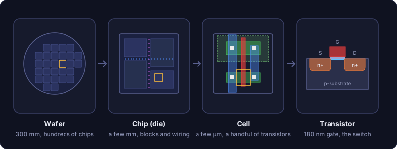
What is a chip, really?
A chip is a small piece of silicon with millions to billions of transistors on it, wired together by several layers of metal. Each transistor is a tiny voltage-controlled switch. Put switches together and you get logic gates; put gates together and you get adders, memories and processors. Put a few transistors together carefully and you get amplifiers, filters and data converters, the analog circuits that connect chips to the real world.
The picture above zooms in four steps:
| Level | Size | What you design there |
|---|---|---|
| Wafer | 300 mm | Nothing: the factory (fab) prints hundreds of copies of your chip on it |
| Chip (die) | a few mm | The floorplan: where the blocks go and how power and signals reach them |
| Cell | a few µm | A gate, a memory bit or an amplifier: a handful of transistors and their wiring |
| Transistor | ~100 nm | Its width W and length L, the two numbers a circuit designer chooses |
Full-custom design, the kind IC Studio is built for, works at the cell and transistor level: you choose every transistor and draw (or generate) every shape.
How a chip is designed
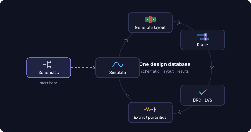
- Specification: what the circuit must do. “Invert a 1.8 V signal in under 50 ps”, “amplify by 10 up to 30 MHz”.
- Schematic: the circuit as symbols and wires: which transistors, how big, connected how.
- Simulation: a SPICE simulator solves the circuit’s equations and shows you voltages and currents, before anything is built.
- Layout: the circuit drawn as the coloured polygons the factory turns into masks, one per layer of the manufacturing process.
- Verification: DRC checks the drawing follows the factory’s design rules; LVS checks the drawing is the same circuit as the schematic.
- Parasitic extraction: the real wires add resistance and capacitance. They are extracted from the layout and put back into the simulation to see their effect.
- Tape-out: the verified layout is sent to the fab as a GDSII file. Weeks later, chips come back.
Steps 2 to 6 repeat until the specification is met. IC Studio keeps all of them on one design database, so going round the loop is a few key presses.
The course
Circuits in ten minutes
Voltage, current, resistors, capacitors, the RC time constant, frequency response and decibels. Read a SPICE netlist.
The MOSFET
How a transistor works: silicon, doping, the channel, threshold voltage, the triode and saturation regions and the square law.
CMOS logic
Transistors as switches: the inverter, NAND and NOR, the transfer curve, delay and power, and how to size transistors.
Hands-on: design an inverter
Draw the schematic, simulate it, measure the switching point and the delay, and size the PMOS to balance it.
From circuit to silicon
How chips are made layer by layer, what layout layers mean, design rules, and where parasitics come from.
Hands-on: lay out the inverter
Generate and route the layout, run DRC and LVS, simulate with parasitics and export GDSII.
Analog building blocks
Small-signal thinking: gm and ro, the common-source amplifier, gain and bandwidth, current mirrors and the differential pair.
Hands-on: an amplifier
Bias and simulate a common-source amplifier, read its gain and bandwidth from a Bode plot, and explore the OTA demos.
A glossary explains every term used in the course, with pointers for further reading.
How to use the course
- Read in order if you are new to the field. Each chapter takes 15 to 30 minutes. The hands-on chapters take about as long in the app.
- Keep IC Studio open next to the text (Installation). Every theory chapter ends with a “Try it” box that opens a demo cell so you can see the idea in a simulation straight away.
- Do the exercises. Changing one number and predicting what will happen before you
press
F5is the fastest way to build intuition. - Everything uses the generic 180 nm technology that new projects start with. It is illustrative, not a real foundry process, but its numbers are realistic: a 1.8 V supply, a 180 nm minimum gate length and a threshold voltage of 0.45 V.
Numbers in this course are real. Every value quoted (switching thresholds, delays, gains) was simulated with IC Studio’s built-in engine on the generic technology, so you should see the same numbers on your screen, give or take the last digit.
Ready? Start with Circuits in ten minutes, or jump straight to the MOSFET if you know your Ohm’s law.